- Homepage
- Key Information
- Students
- Staff
- PGR
- Health and Safety
- Computer Support
- National Student Survey (NSS)
- Intranet Help
Prof Monica Craciun
Research areas
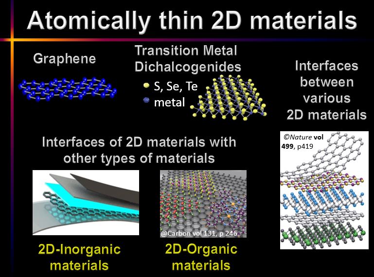
We are working with atomically thin two-dimensional (2D) materials, which are the thinnest materials that can be conceived. Graphene -a monoatomic carbon layer- is the strongest known material, the best electrical and thermal conductor which is mechanically flexible and transparent. Other emerging 2D materials, such as dichalcogenides (WS2, MoS2), have complementary characteristics to graphene such as semiconducting properties necessary for the active parts of electronic and opto-electronic applications. We engineer these materials to enhance their performance and we also use them in 2D heterostructures, as well as in combinations with other organic and inorganic materials in novel emerging technologies.
2D materials engineering
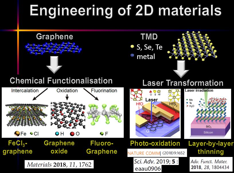
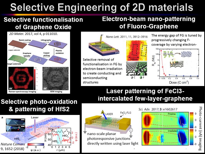
We are engineering the 2D materials by chemical functionalization and laser transofrmation to enhance their properties to unprecedented levels. This process can be achived both on large scale or in a selective way using various nano-patterning strategies.
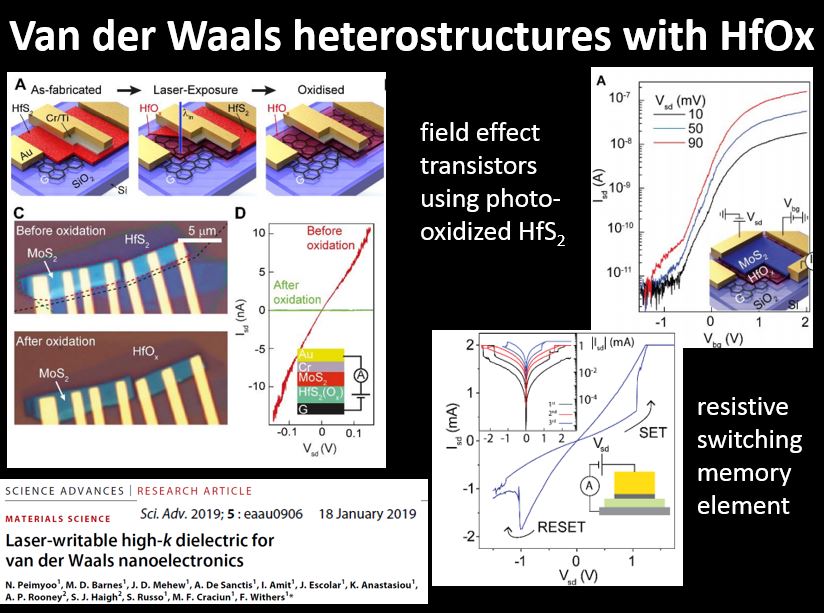
Contributions to this area include novel techniques to pattern electrical circuits in Fluorine- functionalised graphene, of use for whole-graphene electronics [Nano Lett. 11, 3912 (2011)], a method to tailor the band gap of fluorinated graphene by tuning the Fluorine coverage [Nanoscale Res. Lett. 6, 526, (2011) & New J. Phys. 15, 033024 (2013)]. We developed the GraphExeter material (i.e. few-layer graphene intercalated with FeCl3), the best carbon-based transparent conductor [Adv. Mater. 24, 2844 (2012)], with resilience to extreme conditions [Nature Sci. Rep. 5, 7609 (2015)], as well as its laser pattering to define photoactive interfaces. In terms of laser modification of 2D materials, we contributed to the development of a method to accurately produce MoTe2 layers and control their thickness for electronics and optoelectronics [Adv. Funct. Mater. 28 1804434 (2018)]. Our most recent innovation is the development of selective oxidation of 2D materials and of laser-writable high-k dielectric for 2D nanoelectronics [Science Advances 5, eaau0906 (2019)].
Atomically thin optoelectronic devices
The exploitation of 2D materials with extraordinary performances in optoelectronic devices such as photodetectors, solar cells, light emitting devices is at the heart of this research. In particular, the development of mechanically flexible display and conformable products is an essential step in the effort to develop next-generation opto-electronics technologies.
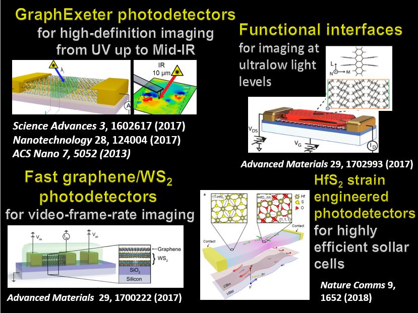
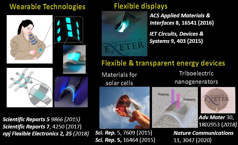 Advances in chemical functionalization have shown that the properties of 2D atomically thin materials can be enhanced to unprecedented levels by chemical functionalization. An example of the potential of chemical functionalization is GraphExeter, a graphene-based material which my team developed at Exeter. In this case, functionalization with FeCl3 of few-layer graphene results in the best transparent electrical conductor which outperforms Indium Tin Oxide used in displays and solar cells. For example, we demonstrated the potential of GraphExeter for flexible and transparent electronics [Nature Sci. Rep. 2015, ACS Nano 2013], wearable electronics, foldable light emitting devices [ACS Appl. Mater. Int. 2016] and solar cells.
Other advances from our group in this field include photodetectors such as the demonstration of 2D heterostructures for video-frame-rate imaging applications [Adv. Mat. 2017], the intelligent design of 2D devices [Adv. Mat. 2017], engineering of organic-semiconductor-graphene phototransistors amplified imaging at ultralow light levels [Adv. Mat. 2017] and functionalized graphene photodetectors for high-definition sensing and video technologies [Science Advances (2017)]. In the area of photovoltaics we demonstreated the development of the first electron funnel on a chip needed for the next generation of efficient solar cells [Nature Communications (2018)].
Transparent & flexible electronics
The development of optically transparent and mechanically flexible electronic circuitry is an essential step in the effort to develop next-generation electronics technology.
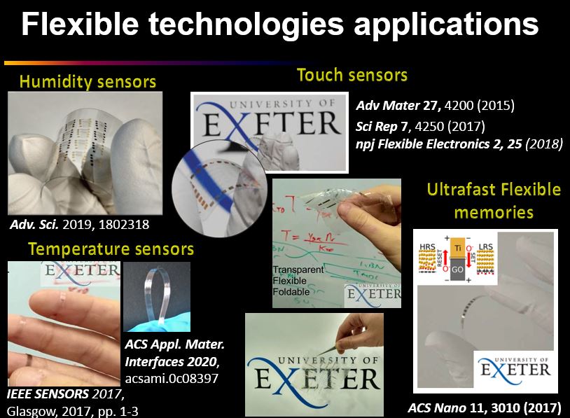
Graphene has a variety of properties which make it an ideal material for such applications: the thinnest, the strongest and yet flexible transparent material, an outstanding electricity and heat conductor with remarkable stiffness and lightness. In particular, graphene is an ideal material for various electronic devices, chemical and biological sensors, and for making the transparent conducting electrical contacts in touch-sensitive screens. Using graphene we have demonstrated graphene-based transparent and flexible touch sensor as well as other types of sensors such as humidity and temperature sensors.
One of the main advantages of 2D materials for various applications is that they can be prepared in form of water-based solutions. The high yield and cost-effectiveness of this method make them of great interest for printed electronics, composites, and bio- and healthcare technologies. Our developments in this area include the integration of high‐quality graphene films obtained from scalable water processing approaches in emerging energy harvesting devices [Adv. Mater. 30, 1802953 (2018)], opening new possibilities for self-powered electronic skin, flexible and wearable electronics. Building on this work, we developed a method for the fabrication of micrometer-sized well-defined patterns in water-based 2D materials [Adv. Sci. 6, 1802318 (2019)]. This method was used to create humidity sensors with performance comparable to that of commercial ones. These sensor devices are fabricated onto a 4 inch polyethylene terephthalate (PET) wafers to create all-graphene humidity sensors that are flexible, transparent, and compatible with current roll-to-roll workflow.
Wearable electronics & smart textiles
We are establishing new technologies for flexible, transparent, comfortable and easy to carry textile-embedded electronic devices. Graphene materials are emerging systems for wearable electronics and smart textiles applications due to their exceptional properties such as electrical conductivity, optical transparency and mechanical flexibility. These properties offer opportunities for the seamless incorporation of electronic devices in textiles, unlocking a future where interacting with electronic devices will be as simple as getting dressed.
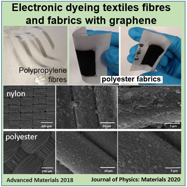
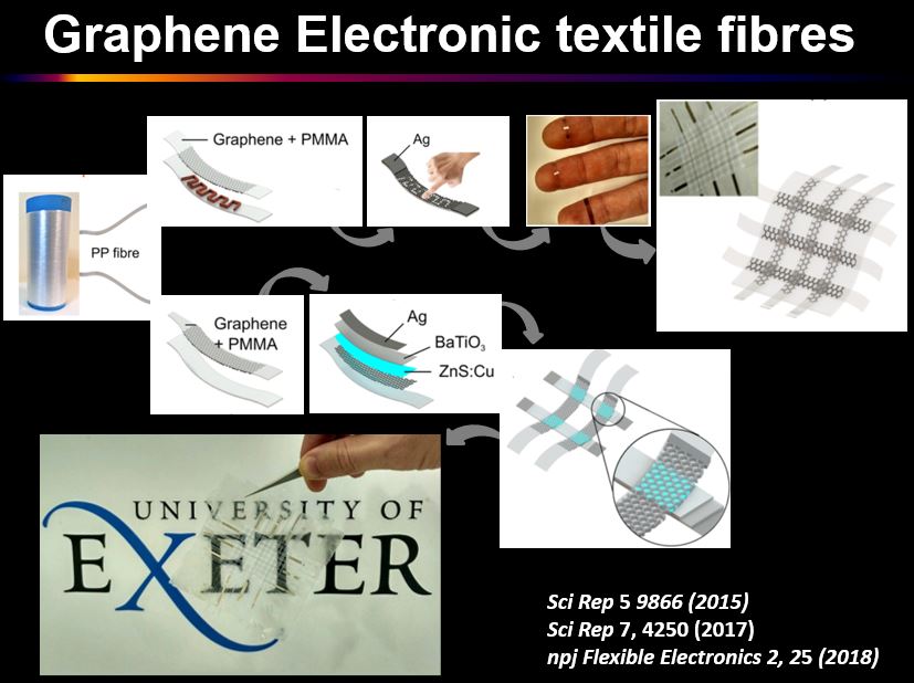 One approach that we follow is to build electronic devices on textile fibres. Our devices combine organic and inorganic semiconductors and dielectrics with graphene as conductive layer, in a novel concept that merges flexibility, transparency, optoelectronic properties and fabrication compatibility of these materials with textiles. All electronic devices need wiring, so the first issue to be addressed is the development of conducting textile fibres which keep the same aspect, comfort and lightness. We have pioneered a new technique to embed transparent, flexible graphene electrodes into fibres commonly used in the textle industry [Nature Sci. Rep. 2015], [Nature Sci Rep. 2017]. The methodology that we have developed to prepare transparent and conductive textile fibres by coating them with graphene has opened a way to the integration of electronic devices on these textile fibres.
These graphene-based conductive fibres were used as a platform to build integrated electronic devices directly in textiles. For example, we demonstrated graphene electronic textile fibers that function as touch-sensors and light-emitting devices [npj Flexible Electr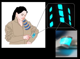 onics 2, 25 (2018)].
We also demonstrated the weaving of such graphene electronic fibres in a fabric which enabled the realization of pixels for displays and position sensitive functions. Finally, we recently demonstrated the use of graphene-coated polypropylene (PP) textile fibers as temperature sensors within a low-operating voltage carbon–graphene e-textile system [ACS Appl. Mater. Interfaces 12, 26, 29861 (2020)].
For the development of fabric-based wearable devices, one of the critical challenges is the seamless incorporation of electronics in textiles that will preserve their softness and comfort.
A key feature is the realisation of electrically conductive coatings on textile that conform to the irregular and coarse structures of the textile fabrics. Therefore, a different approach compared to fibers is needed for creating conductive textile fabrics without compromising the properties of the fabric.
We recently demonstrated a simple, low-cost, efficient, and highly scalable method of ultrasonic spray coating for coating three types of textile fabrics, meta-aramid, polyester and nylon, with a water based graphene nanoplatelets suspension [J. Phys. Mater. 4 014004 (2021)]. These conductive textile fabric electrodes show a sheet resistance as low as 4.5 kΩ/sq without any intentional doping or required additives for improved adhesion. Such fabric electrodes have applications in sensors or energy-harvesting wearable technologies.
Quantum Phenomena & Nano electronics
We use nano-electronic devices to investigate the electronic structure of graphene and functionalized graphene materials. Our work spans from fundamental studies in graphene such as Quantum Transport, Quantum Hall Physics and Weak localization studies to applications of these materials in photodetectors, p-n diodes, transistors and resistive memories.
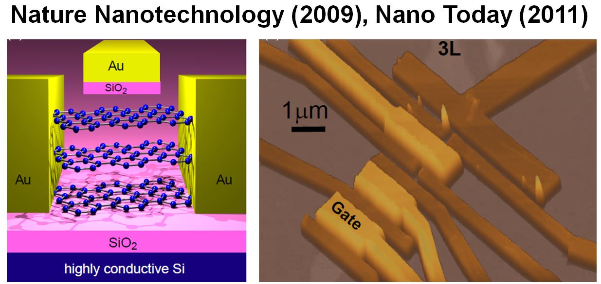
Contributions from our group include the first experimental demonstration of charge carriers propagation in monolayer graphene via evanescent waves [Phys. Rev. Lett. 100, 196802 (2008)] and the discovery that ABA-stacked trilayer graphene is the only gate-tuneable semimetal [Nature Nanotech. 4, 383 (2009)], opening the research area of few-layer graphene (FLG). We also published the first experimental evidence that trilayer graphene has a unique stacking-dependent quantum Hall effect [Phys. Rev. B(R) 84, 161408 (2011)], the first studies of electrical transport in FLG with record high charge densities controlled by liquid ionic gating [PNAS 108, 13002 (2011)], and the first direct observation of the electric field tuneable energy gap in ABC-stacked trilayer graphene [Nano Lett. 15, 4429 (2015)]. Other advances are the realisation of a highly efficient graphene Cooper pair splitter device for quantum information processing [Nature Sci. Rep. 6, 23051 2016], and revealing the mechanism of large distance supercurrent propagation through graphene-superconductor junctions [Nano Lett. 16, 4788 (2016)]. We also developed novel ways to strain graphene [Nano Lett. 14, 1158 (2014)] which were used to experimentally study electron states in uniaxially strained graphene [Nano Lett. 15, 7943 (2015)], of interest for straintronics applications. Recently, we probed different strain configuration in 2D superlattices and provided a new mechanism to induce complex strain patterns in 2D materials [Nano Lett. 18, 7919 (2018)], with profound implications in the development of future electronic devices based on heterostructures
Our most recent advances is the development of laser-writable high-k dielectric for 2D nanoelectronics [Science Advances 5, eaau0906 (2019)].
Similar to silicon-based semiconductor devices, van der Waals heterostructures require integration with high-k oxides. We demonstrated a method to embed and pattern a multifunctional few-nanometer-thick high-k oxide within various van der Waals devices without degrading the properties of the neighboring two-dimensional materials. This transformation allows for the creation of several fundamental nanoelectronic and optoelectronic devices, including flexible Schottky barrier field-effect transistors, dual-gated graphene transistors, and vertical light-emitting/detecting tunneling transistors. Furthermore, upon dielectric breakdown, electrically conductive filaments are formed. This filamentation process can be used to electrically contact encapsulated conductive materials. Careful control of the filamentation process also allows for reversible switching memories.

